At a scale far smaller than a grain of dust, researchers have done something that once sounded almost impossible: they have trapped infrared light inside an engineered atomic lattice just 42 nanometers thick. That is roughly 2,000 times thinner than a human hair, and thinner still than the faintest film of paper.
The achievement comes from a team at the University of Warsaw in Poland, and it matters for more than just the elegance of the physics. When light can be controlled in such tiny spaces, the door opens a little wider for compact photonic devices, ultrafast communication systems, and perhaps even a future where electronics rely more on photons than on electrons.
A tiny structure with a very big job
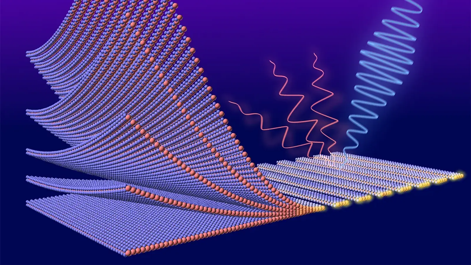
The material at the heart of the experiment is molybdenum diselenide, usually shortened to MoSe2. It belongs to a family of ultrathin materials called transition metal dichalcogenides, or TMDs, which have attracted intense interest because of their unusual optical and electronic properties.
In this case, the researchers used a layered arrangement of molybdenum and selenium atoms to create a nanometre-scale grating that could hold infrared light in place. The secret is the material’s exceptionally high refractive index, which means it can bend and slow light more effectively than many other substances. That slowing effect is crucial when the goal is to confine light rather than let it pass through.
Infrared light is especially tricky to manage because its wavelength is longer than visible light. The longer the wavelength, the harder it becomes to squeeze that light into a very small structure without losing control of it. Pushing past that limit requires not just a clever design, but almost surgical precision.
How the team built the trap
To make the MoSe2 layers, the team turned to molecular beam epitaxy, a manufacturing method that grows crystals atom by atom in an ultra-controlled vacuum environment. Think of it as atomic-scale printing. After growing the sheets, the researchers carved microscopic stripes into them, leaving gaps smaller than the wavelength of the infrared light they wanted to confine.
Those subwavelength gaps are essential. They help form the conditions needed for a phenomenon known as a bound state in the continuum, or BIC. The phrase sounds contradictory, and in a way it is. A BIC is a state in which light stays trapped inside a structure even though it exists alongside other light waves that would normally radiate away.
That strange balance is what makes the result so useful. It allows light to be confined without the usual escape routes, provided the structure has been designed with exceptional accuracy. Before building the device, the researchers carefully modeled the grating to make sure the geometry would support this behavior.
According to the team’s paper, they used the strong refractive index of MoSe2 to design and fabricate subwavelength gratings capable of hosting BICs. In plain terms, they found a way to make a material not just carry light, but hold onto it.

Why this matters for photonics and computing
The immediate significance lies in photonics, the field that uses light to carry and process information. If light can be trapped and manipulated at extremely small scales, engineers can build flatter, denser, and potentially faster devices for lasers, wavefront control, sensing, and signal processing.
The longer-term dream is optical computing. Instead of relying solely on electrical current moving through metal-based circuits, optical systems would use photons. That could reduce heat, increase speed, and shrink components dramatically. It is still a long road. Plenty of obstacles remain, from manufacturing consistency to integration with existing hardware. But experiments like this show that the physics itself is not the roadblock it once seemed to be.
There is also a practical engineering challenge that should not be overlooked. The MoSe2 sheets in this study were not flawless straight out of production. The team had to polish them with silk tissues to remove irregularities. That detail may sound modest, but it tells the real story of nanoscience: progress often depends on painstaking refinement, not dramatic breakthroughs alone.
Even so, the researchers are optimistic that the method can be improved and adapted to other TMD materials. If that happens, the approach could become a broader platform for nanoscale light control, not just a one-off demonstration.
Expert Insight
“What makes this result exciting is not simply that light was trapped, but that it was trapped in a material system small enough to matter for future devices,” says Dr. Elena Markovic, a fictional photonics researcher. “We are seeing the kind of precision that could eventually support ultracompact lasers, advanced sensors, and integrated optical circuits. The challenge now is turning a laboratory success into a reproducible technology.”
That is the real edge of this work. It is not a finished product, and it is not meant to be. It is a proof that the rules of light can be bent with enough care, enough modeling, and enough control over matter at the atomic level. And in the race to make smaller, faster, more efficient technology, that is no small thing.

“The cosmos has always fascinated me. I write about space missions, astronomy, and the technologies pushing humanity beyond Earth.”

Discussion
Leave a Comment