3 Minutes
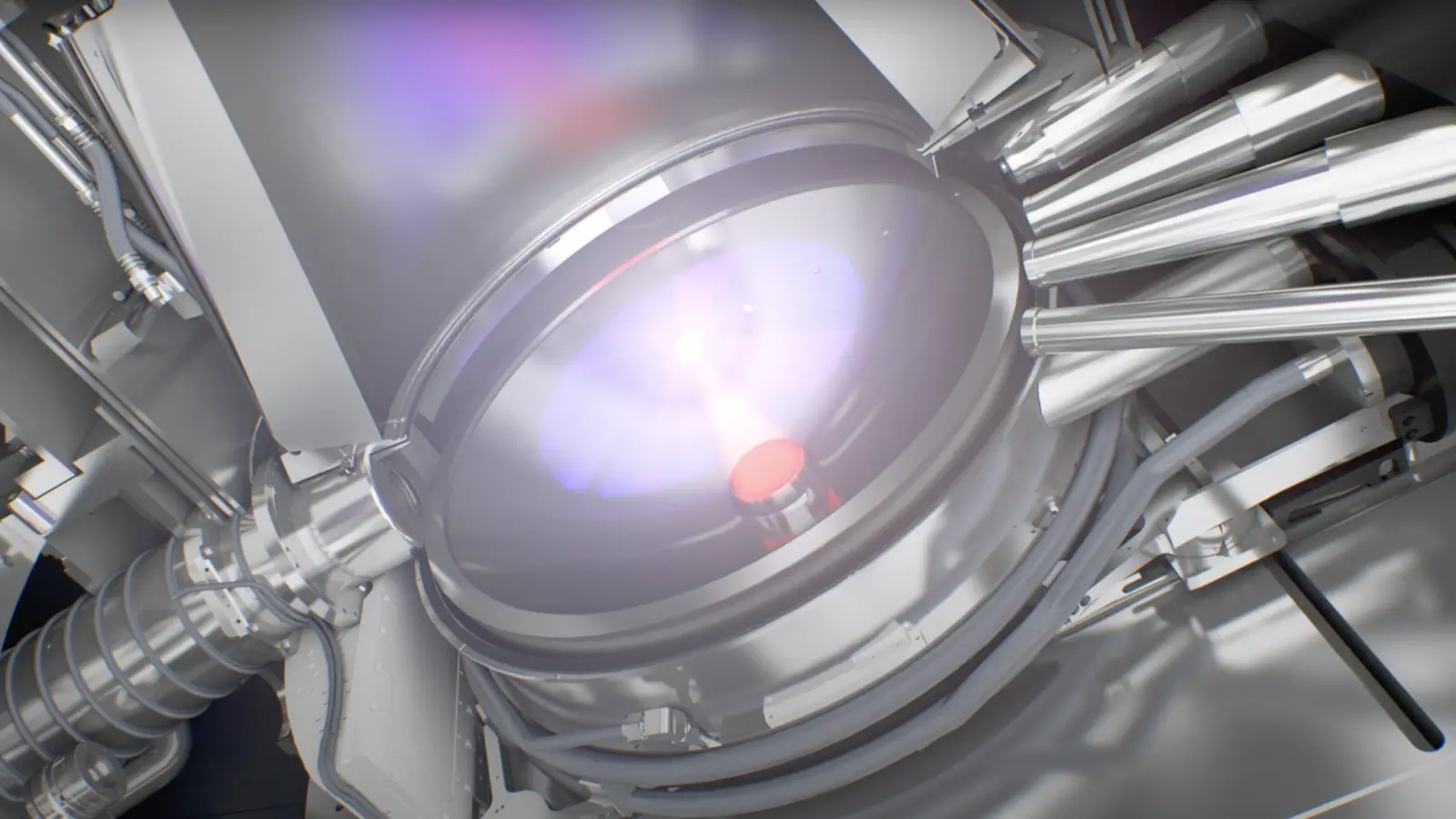
Chinese engineers have reportedly built a working extreme ultraviolet (EUV) lithography prototype, a development that could accelerate Beijing's push for semiconductor independence and unsettle global chip supply dynamics.
Why this matters: a potential shift in the semiconductor race
According to a Reuters report, the prototype is generating UV light for wafer etching and is already functional in some capacity. That alone is a milestone: EUV systems are the most complex machines in chipmaking, and until now the market has been dominated by the Dutch firm ASML. If China can move from a prototype to production machines, it would dramatically narrow a critical technological gap.
There are caveats. Sources say China has been cannibalizing older ASML units for parts and components, and the prototype has not yet taped out a finished chip. Still, the pace of progress is striking — faster than many analysts expected — with some insiders predicting EUV could become common in China by around 2030. That timeline would shave years off previous estimates and shift strategic calculations in Washington and Taipei.

What we still don’t know
- Key technical details are missing: the exact light source, optics, and throughput numbers remain unconfirmed.
- Integration and yield are unresolved: a working light source is only one step toward regular, high-yield production.
- Supply chain questions linger: continued dependence on salvaged ASML parts shows China is not yet fully self-reliant.
Why do these gaps matter? Because an EUV machine that emits light is not the same as an EUV tool that reliably machines cutting-edge nodes at scale. Tape-out — the process of completing a chip design and sending it to fabrication — is the real test. Until a Chinese system produces functioning, high-yield chips, many technical and commercial hurdles remain.
That said, the broader context helps explain the urgency. AI-driven demand has sharply increased pressure on domestic chip capacity, pushing companies like Huawei to partner with local foundries such as SMIC. Beijing has poured resources into talent, reverse engineering, and industrial ecosystems to reduce reliance on foreign suppliers. SMIC's own advances, including its N+3 roadmap meant to rival mainstream 5nm-class processes, are part of that same drive.
For now, the industry will be watching for proof: will China publish test wafers? When will the prototype tape out its first chips? And critically, how much of the machine still depends on legacy ASML components? Answers to those questions will determine whether this is a symbolic milestone or the start of a real shift in global semiconductor power.
Source: wccftech


Leave a Comment