
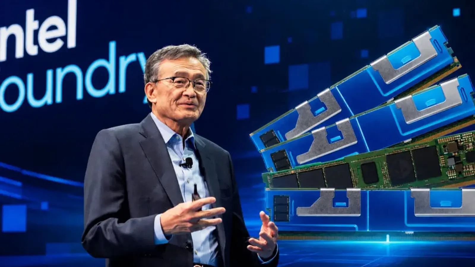
Intel is reorganizing to become a choice supplier for custom chip makers, shedding layers of internal bureaucracy and pursuing new product categories across advanced process nodes. The company is targeting the hot ASIC market and advancing packaging and memory technologies while recruiting senior industry executives to accelerate those efforts.
Leadership moves and the ASIC strategy
Intel has hired Din Jarnak, a former Marvell executive, as part of a broader push into ASIC design and custom silicon services under CEO Lip-Bu Tan. Industry analyst Jack Gold says Intel likely put Jarnak in place to win the contracts required to expand the companys footprint in the ASIC market.
Gold added: "Marvell designs chips; therefore, my assumption is that Jarnak has a good understanding of the process, especially of the differences between operating in a chip-design company and a company like Intel that both designs and manufactures its own chips."
The ASIC market has become crowded in recent years with cloud and AI players partnering with established silicon vendors. Reported collaborations include:
- Google designing TPU chips with Broadcom, Marvell, and MediaTek.
- Amazon developing Trainium chips with Marvell.
- Microsoft designing Maia AI accelerators with OpenAI, Marvell, and Broadcom.
- OpenAI unveiling the Jalapeno accelerator with Broadcom.
- Anthropic reportedly developing an ASIC with Broadcom and Samsung.
Intel has already announced some wins in this area. In July the company announced an agreement to design and manufacture a next-generation security processor for Fortinet, intended for high-throughput firewalls and security infrastructure. CFO David Zinsner told investors in July that Intels ASIC business is at an annual run rate near $2 billion and could grow to about $4 billion in the not-too-distant future.
Foveros packaging and a potential Nvidia opportunity
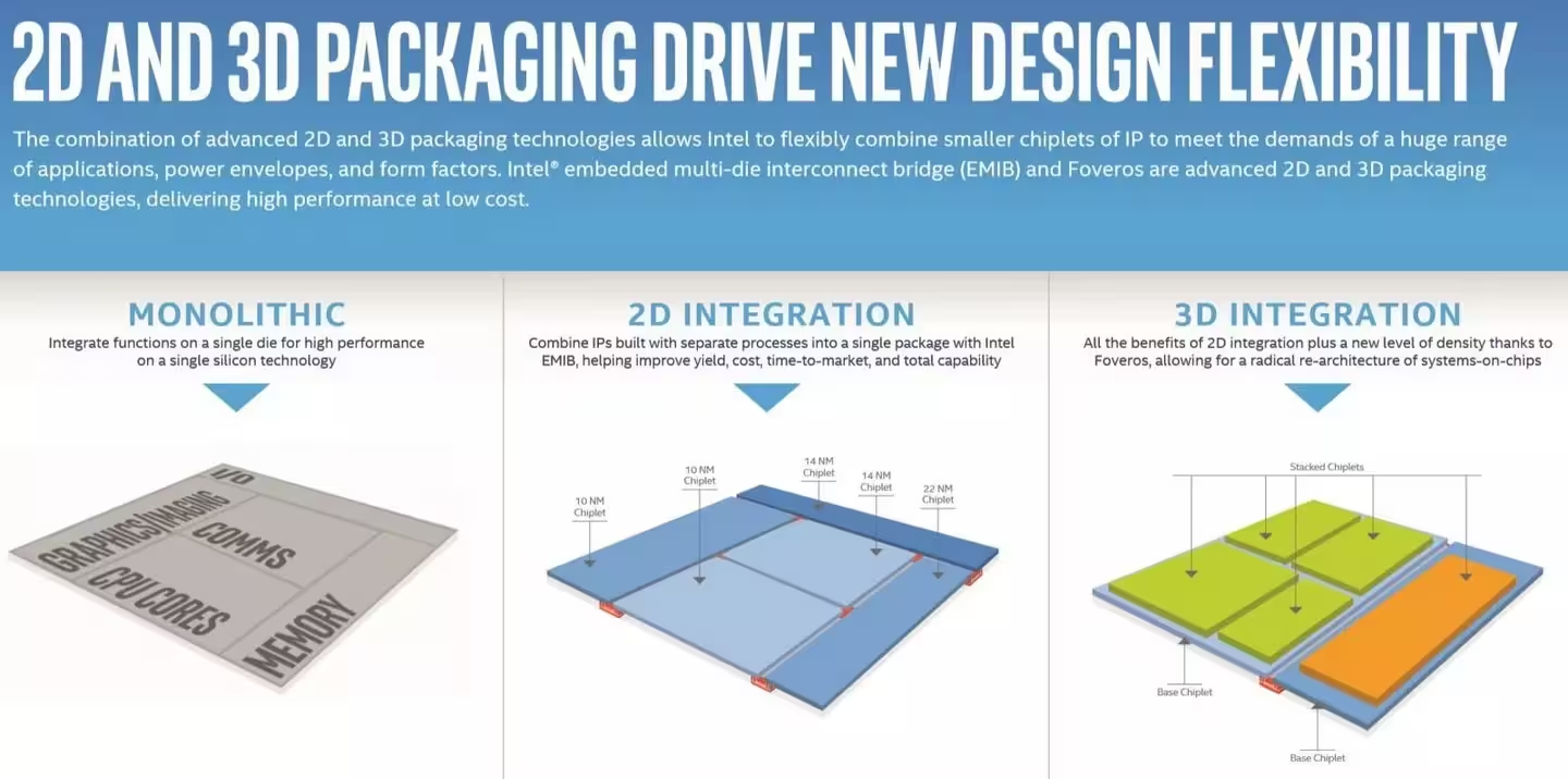
Reports today indicate Nvidia may use Intels Foveros advanced packaging technology in 2028, a development that would represent a significant commercial opportunity for Intel if realized. Foveros enables true three-dimensional stacking of active dies. Dies can be placed face-to-face or back-to-back directly on a base die or interposer layer, enabling very high interconnect density and shorter vertical signal paths that reduce latency. The process relies on hybrid copper-to-copper bonding.
Foveros is positioned as an advancement over Intels EMIB approach. EMIB connects multiple smaller silicon chiplets inside a package using small silicon bridges embedded in the organic package substrate, with high-density interconnects concentrated where chiplets meet the silicon bridge. EMIB-T moves that concept forward by embedding through-silicon vias, or TSVs, directly into the silicon bridges. Those vertical pathways allow power and high-speed signals to pass from the bottom of the package, through the silicon bridge, and into processors or memory on the upper layers, enabling three-dimensional die stacking.
Memory research and executive hires
Intel is also quietly advancing in memory technologies, working on projects such as XBM and Z-Angle Memory, or ZAM. ZAM is described as a 3D-stacked DRAM architecture that replaces conventional through-silicon vias with slanted or angled connections. That geometry creates a central thermal column to aid heat dissipation, uses hybrid copper-to-copper bonding, and omits traditional capacitors to increase density.
At its recent financial meeting Intel specifically referenced hiring Sho-Chi Li, the former CEO of SK hynix, signaling that the companys memory ambitions may be part of a broader plan to expand advanced businesses and strengthen manufacturing capacity. CEO Lip-Bu Tan has repeatedly preferred bringing experienced external executives into key roles as a way to move away from Intels traditional promotion-from-within model and to accelerate organizational change.

“I love exploring gadgets, apps, and trends that redefine how we connect, work, and play in a digital world.”

Discussion
Leave a Comment
Comments
No comments yet. Be the first.