
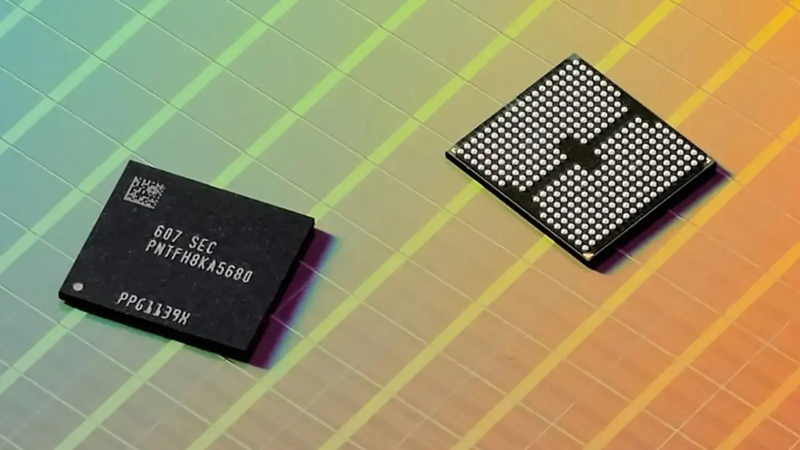
In a bustling Santa Clara hall, Samsung quietly lifted the curtain on hardware that feels less incremental and more like a small revolution. Engineers crowded around glass cases. Cards were swapped. The takeaway was blunt: memory is changing its shape.
The headline: BV-NAND V10. This is bonded V-NAND pushed to a new extreme, with more than 400 stacked layers built using Samsung's advanced bonding techniques. The result is not just a taller pile of silicon. It delivers about 58% higher density versus the previous generation, and that extra vertical real estate translates directly into faster reads, quicker writes, improved I/O, and measurable power savings. Short version: denser memory that eats less energy while moving data faster.

Stack it up and shrink the gap
Now imagine memory that sits literally on top of the processor. Strange? Powerful. Samsung calls that zHBM. It borrows the wafer bonding playbook and applies it to high bandwidth memory, redesigning the physical relationship between DRAM and accelerator. Instead of being a neighbor across the board, zHBM is stacked above AI accelerators, slashing the distance data must travel. Latency falls. Speed climbs. Power use drops.
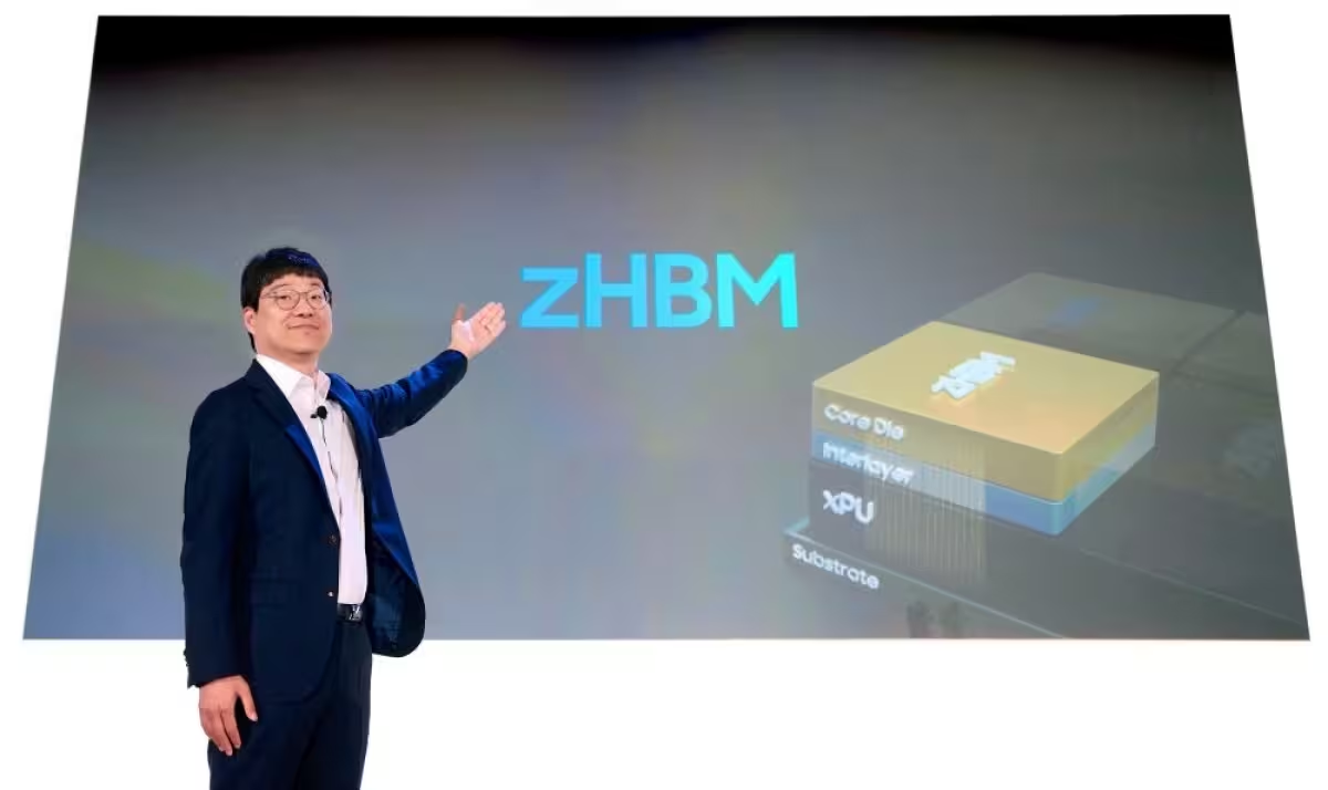
Samsung says zHBM can deliver roughly eight times the performance of the upcoming HBM5 standard while offering around ten times the memory density and about three times the energy efficiency. Those are big claims. They hinge on two things: extremely tight vertical integration and the company's wafer bonding expertise. If real-world systems match those numbers, zHBM could reshape how datacenters and AI racks are architected.

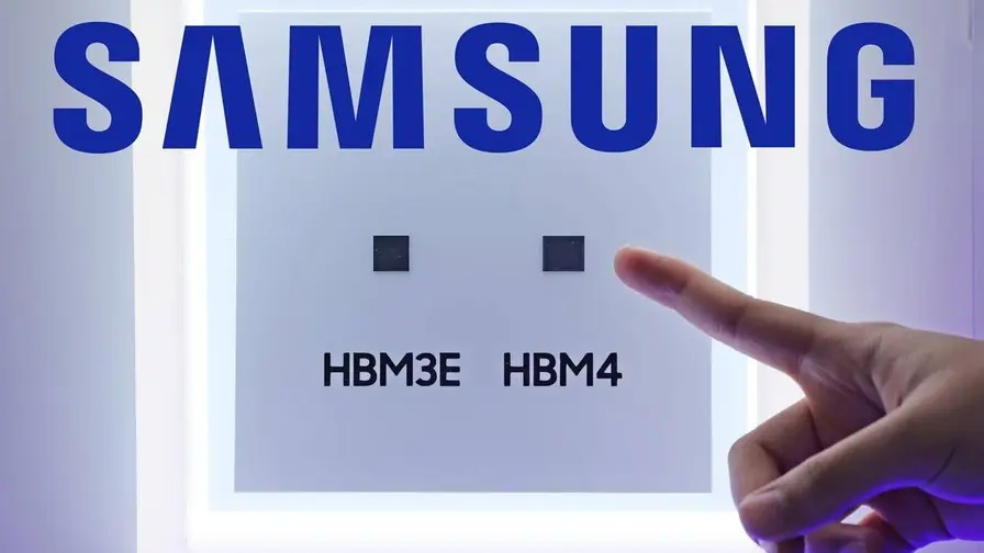
Samsung also displayed its progress on industry-standard HBM: HBM4E samples have already been shipped to customers, and the company presented HBM5 as the next baseline for high bandwidth memory. But zHBM is positioned as the faster, more compact, and more power-savvy option for workloads that demand scale.
Not every advance is aimed at the cloud. Enter zNAND-O, a next-generation flash derived from V-NAND methods but tuned for edge AI. Samsung is developing 4 and 8 layer versions that promise tighter space efficiency, better I/O performance, and lower latency than conventional NAND. Think of zNAND-O as a lean, local cache for AI inferencing close to the user, with zHBM reserved for heavy lifting in training and large-scale inference back in the cloud.
There was one more neat piece: LPDDR5X-PIM. This is the industry’s first LPDDR that integrates Processing-In-Memory features, performing some compute inside the memory before data ever leaves. The effect is straightforward: less data shuttled back and forth, higher effective bandwidth, and better energy numbers. In workloads where simple transforms or reductions dominate, PIM can cut bottlenecks without changing the whole software stack.

The morning keynote framed the strategy. Jin-Yub Lee, Executive Vice President and Head of Flash Product & Technology, together with Kyungryun Kim, Vice President and Project Leader of the DRAM Design Team, sketched Samsung's view of memory as an active system element, not just passive storage. They argued that stacking and bonding will be the levers to wring more performance and efficiency from AI systems.
So where does this leave us? Samsung showed a toolbox: denser flash for storage, stacked HBM variants for bandwidth-hungry compute, compact NAND for edge AI, and RAM that can do work. Each piece matters. Put together, they hint at a future where memory design plays the starring role in taming AI's resource hunger.

“I love exploring gadgets, apps, and trends that redefine how we connect, work, and play in a digital world.”

Discussion
Leave a Comment
Comments (2)
Feels like big promises, numbers sound juicy but where's the testing? zHBM sounds neat, but software thermal packaging headaches remain, we'll see
wow, 400 layers? ok thats wild, if real this could flip the datacenter game. power savings + density? skeptical but hyped. demo pics pls