
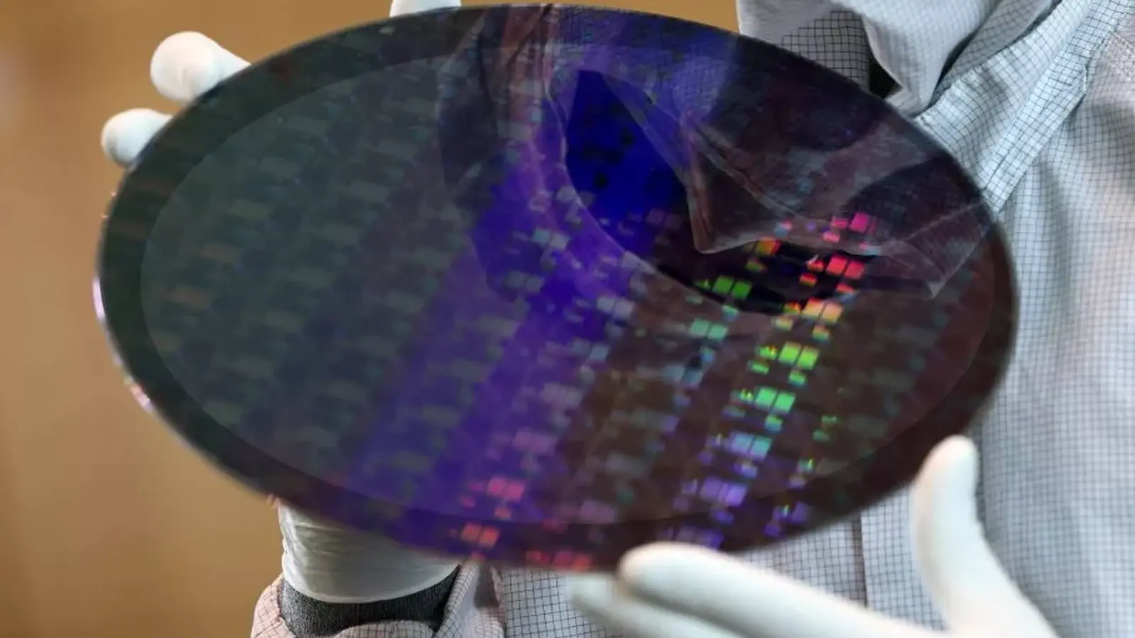
Imagine a channel layer so thin it measures in fractions of a single nanometer. Tiny changes at that scale decide whether the transistor will hum or stall. TSMC, working with Taiwan's NYCU, didn’t chase exotic new materials. They rewired the transistor's surface chemistry instead.
Why a wafer-thin aluminum layer changes the rules
Modern chips pack billions of transistors using 3D designs like FinFETs and gate-all-around FETs. Those architectures boost gate contact area by wrapping the gate around a raised channel. The trick works—until the channel gets vanishingly thin. As channels shrink toward 3 to 5 nanometers, gate control weakens. Go below roughly 3 nanometers and electrons start interacting with gate materials in ways that raise resistance and leak current.
That’s where single-layer, two-dimensional semiconductors such as molybdenum disulfide (MoS2) look appealing. At about 0.7 nanometers thick, a MoS2 channel promises much better electrostatic control and lower leakage, letting manufacturers aim for sub-1nm gate stacks and ultra-short channel lengths. But ultra-thin also means ultra-fussy. Try to deposit a gate dielectric the old way and you get a rough, patchy layer that undermines performance.

TSMC and NYCU turned the problem inside out. Instead of inventing a brand-new dielectric or forcing aggressive deposition chemistry onto MoS2, they engineered the channel surface first. The team deposited an epitaxial aluminum monolayer on MoS2 and let it oxidize into a uniform aluminum oxide only 0.42 nanometers thick. On top of that micro-thin buffer, they placed a high-k hafnium oxide dielectric.
The result: a remarkably smooth gate interface that tames leakage and sharpens control over electron flow. In tests, the surface-engineered stack delivered gate control and lower resistance comparable to having a roughly 1 nanometer dielectric, but with the channel benefits of MoS2.

There are clear highs and practical questions. Manufacturing at scale still demands repeatable, clean epitaxy and integration into back-end processes. Still, this approach sidesteps a lot of the material tradeoffs chipmakers have been wrestling with and offers a pragmatic path toward denser, faster logic devices.
This surface-engineering move could be the practical bridge to mass-produced sub-1nm transistors and a new chapter in semiconductor scaling.


“I love exploring gadgets, apps, and trends that redefine how we connect, work, and play in a digital world.”

Discussion
Leave a Comment
Comments
No comments yet. Be the first.