
Imagine removing a single atomic layer without touching what lies beneath. That kind of precision sounds like laboratory wizardry. Yet researchers at Princeton and the U.S. Department of Energy laboratories have sketched a path toward that exact control, using a subtle chemical pre-treatment to change how plasma interacts with ultrathin materials.

Researchers have created a new plasma-based manufacturing approach that could improve the precision of semiconductor fabrication. The breakthrough may enable smaller, faster, and more energy-efficient computer chips as the industry pushes beyond today’s manufacturing limits.
Silicon has driven decades of progress in electronics, but the material is approaching practical limits in size and performance. To squeeze more capability into a chip, engineers are turning to atomically thin materials that can partner with silicon in future transistors. One standout candidate is molybdenum disulfide, known in materials science by the formula MoS2. Three atoms thick. Compact. Promising.
How a tiny chemical layer shifts the odds
MoS2 belongs to a family called transition metal dichalcogenides, or TMDs. Picture a sandwich: a sheet of molybdenum atoms tucked between two layers of sulfur. In advanced device designs, manufacturers may need to remove only the top sulfur layer while leaving the molybdenum and the lower sulfur layer intact. That is a knife-edge problem. Too much energy, and the underlying atoms are damaged. Too little, and the top layer stays stubbornly attached.
.avif)
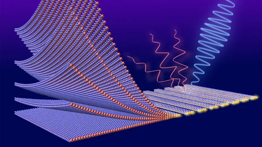
A frame from a simulation video shows a plasma ion (purple) dislodging atoms from a class of extremely thin materials called transition metal dichalcogenides (TMD). This material might be an ideal replacement for silicon in computer chips. A layer of molybdenum atoms (blue) is sandwiched between two layers of sulfur (green). The TMD has been coated in oxygen (red) so that when the plasma ion strikes, the sulfur and oxygen bond to form sulfur dioxide. This allows for the removal of the upper layer of sulfur without damaging the molybdenum below.
Traditional plasma etching relies largely on kinetic impacts: ions in the plasma slam into the surface and physically dislodge atoms. But those ion energies are not all identical; they fall across a spectrum. For untreated MoS2, simulations indicate that removing a sulfur atom takes roughly 30 electron volts. That number sits uncomfortably close to the threshold that would harm the molybdenum layer underneath. In real factory conditions, a fraction of ions inevitably spike above that safe margin and inflict damage.
The new approach flips the script by letting chemistry do the heavy lifting. Using first-principles simulations, the team discovered that coating the MoS2 surface with oxygen or fluorine ahead of plasma exposure reduces the energy needed to remove surface sulfur. A fluorine coating can lower the required energy to about 10 electron volts; oxygen brings it down to roughly 14 electron volts. That widening of the operating window means manufacturers can tune plasma conditions to strip only the top sulfur layer with far less collateral harm.
What actually happens when an ion meets a chemically primed surface? The simulations show that the incoming ion can trigger the formation of small, volatile molecules. With oxygen present, two oxygen atoms combine with a neighboring sulfur atom to form sulfur dioxide, which readily desorbs as a gas. Fluorine plays a similar role, producing sulfur-fluorine species that detach more easily than raw sulfur atoms.
That chemical pathway reduces the reliance on brute force. Instead of hoping an ion has just the right energy to knock a sulfur atom free, manufacturers would encourage the surface to transform the sulfur into a removable molecule. The change is small in energy terms but large in manufacturing robustness. A broader energy margin is what turns a finicky lab demonstration into a process that can survive the variability of a fab.
Implications for next-generation semiconductors
Why does this matter beyond a neat lab result? Because selective, nondestructive removal of atomic layers opens design possibilities. Engineers can imagine heterostructures that combine silicon with TMD layers, stacking materials with complementary electrical properties to build transistors that are smaller, faster, or more energy efficient. Chipmakers already face enormous cost and complexity as they push past established lithography limits. Techniques that add precision without extreme thermal budgets or exotic equipment are particularly attractive.

The Princeton-led simulations were published in the Journal of Physical Chemistry Letters, with Yury Polyachenko as the lead author. The paper identifies both the energy thresholds and the chemical intermediates that permit selective processing. The team includes researchers from the Princeton Plasma Physics Laboratory and collaborators who performed high-performance computations at NERSC and Princeton clusters.
The work was supported by the U.S. Department of Energy, including Fusion Energy Sciences and Basic Energy Sciences. The researchers stress that these results come from simulations, so the next steps require careful experimental validation. The immediate follow-ups are straightforward. First, quantify how much lattice damage different process recipes produce, not simply whether damage occurs. Second, test the method across closely related materials, swapping molybdenum for tungsten or sulfur for selenium, to map how broadly the trick works.
Expert Insight
"What excites me is the elegance of using chemistry to widen an engineering tolerance," said Dr. Elena Martínez, a semiconductor process engineer with two decades in wafer-scale fabrication. "This is not about inventing a new plasma gun. It is about nudging surface chemistry so that standard plasma tools can achieve outcomes they could not before. If experiments confirm the simulations, fabs can adopt a relatively simple conditioning step that yields outsized benefits."
Industry adoption will depend on several practical matters: how to apply the oxygen or fluorine functionalization uniformly at scale, how the conditioning affects downstream process steps, and whether any residual species create long-term reliability concerns. Each of those questions is addressable, but they require careful integration work beyond the physics model.
Conclusion
Small chemical edits to a surface can have outsized effects. By lowering the energy barrier for removing a single sulfur layer, oxygen or fluorine functionalization could make plasma processing selective enough for real-world semiconductor production. The result would not be a magic leap but a pragmatic improvement: wider operating windows, lower defect rates, and clearer pathways to combine silicon with atomically thin materials in the devices of tomorrow. The path ahead runs through the lab bench and the fab floor, with simulation guiding experiments and experiments testing manufacturability.


“My work centers on sustainability, energy, and environmental science — examining how innovation can lead to a greener future.”

Discussion
Leave a Comment
Comments (3)
I work with surface treatments sometimes, ive seen small chemical tweaks do wonders, but residuals haunt later steps. eager to see damage metrics and tests on WSe2 etc.
Is this even true? sims are neat but plasma is messy IRL... how do they make oxygen or fluorine coating uniform across wafers? curious, skeptical.
Wow, removing one atomic layer without wrecking the rest? wild science. If O/F pre-treats work in real fabs this could be huge, but lab tests first.