
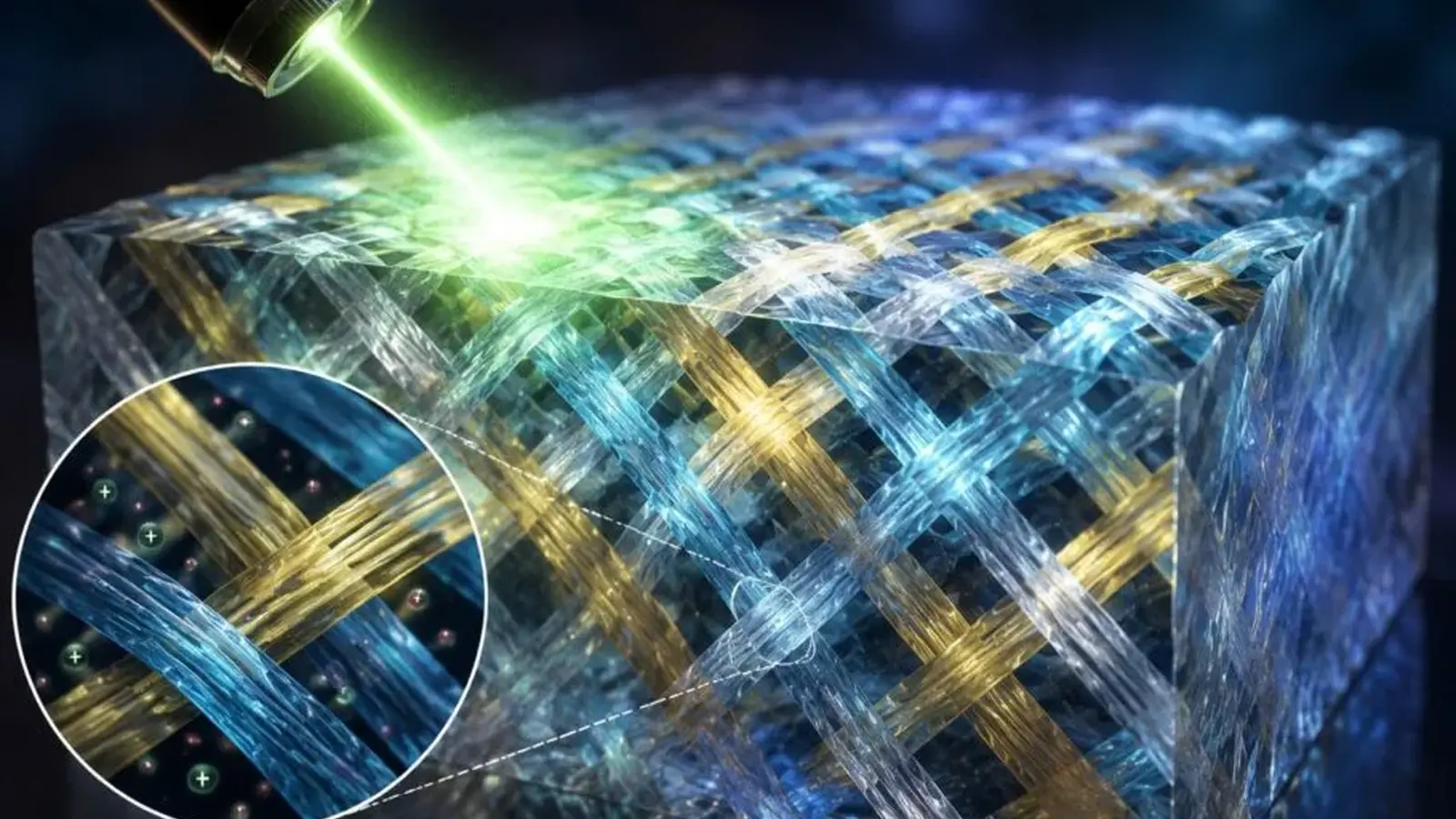
A transparent slab of crystal, chilled to near-freezing, began to rearrange itself. Not in the slow, polite way crystals grow under a microscope, but in a manner that looked almost intentional: filaments of electric polarization rose, crossed, looped and locked into a three-dimensional lattice that resembled woven fabric. The researchers in the lab did not stitch these threads by hand. The material assembled them on its own.
When a material becomes an architect
That spontaneous weaving happened inside a ferroelectric crystal known as KTN:Li, a member of the perovskite family prized for unusual optical and electrical responses. Observers watching the sample through layered imaging techniques expected the familiar patchwork of tiny polarized regions, called domains. Instead they saw long, continuous strands of directed polarization that threaded the interior like yarn in a tapestry. The pattern persisted across depth, not just on the surface. In other words, the crystal produced a true three-dimensional network of electric domains.
Why should anyone outside condensed-matter physics care? Because materials set the limits of technology. Transistors, lasers, solar cells and sensors all trace their lineage to new or better-understood materials. When matter arranges itself into a previously unseen architecture, it opens routes to device concepts engineers have not yet imagined. The discovery of a self-assembled 3D domain network in a solid therefore reads like both a fundamental insight and a materials-design hint: nature sometimes beats us to elegant solutions.

Ferroelectric domains in plain language
Ferroelectric materials host regions where electric dipoles align in a shared direction. Think of each tiny domain as a microscopic arrow pointing one way or the other. When enough arrows align, the region acquires a net electric direction that can be flipped with an external field. That flip-and-hold capability is the reason ferroelectrics are candidates for nonvolatile memory: information can be encoded as polarization states that persist after power is removed.
Domains are not static wallpaper. They form, shrink, merge and reorganize during phase changes, temperature shifts or under applied fields. Usually the patterns are planar or localized. Researchers have characterized vortices, skyrmions and other topological quirks in ferroelectrics before, but a pervasive 3D network of long, interlaced domain filaments is different. It is not merely an exotic curiosity; it signals a mode of ordering that could be robust, addressable and, crucially, manipulable by light.
How the experiment unfolded
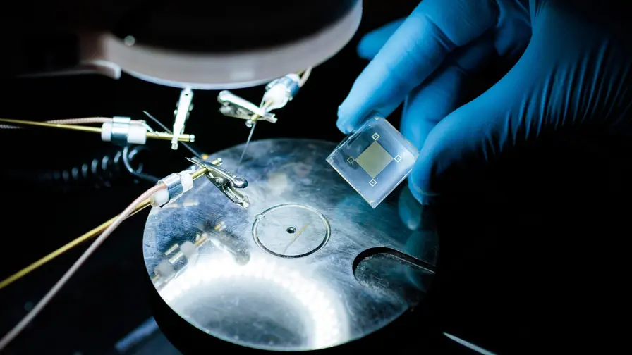
The team worked with potassium tantalate niobate doped with lithium, abbreviated KTN:Li. This perovskite-like compound shows a temperature-driven transition from a high-symmetry paraelectric phase to a low-symmetry ferroelectric phase. The researchers cooled the crystal slowly through that transition while using layered optical and polarization-sensitive imaging to capture the evolution of domain structure in three dimensions.
Initial cooling produced conventional domains. Then, near a critical temperature window, the sample deviated from expectation. Domains near the surface elongated into slender, continuous threads. With further cooling the threads penetrated deeper, intersecting and knotting into a woven lattice. When the team compiled slices of images across depth, the network proved truly volumetric: a repeating, interlaced morphology running through the body of the crystal.

Light as a control knob
Perhaps the most striking experimental result was that focused light altered the woven network. A green laser at 514 nanometers, directed at a region of the sample, caused the interlaced filaments to relax into a simpler pattern within the illuminated volume. Importantly, the effect was not a thermal artifact. Control tests using infrared illumination that delivered comparable heating did not reproduce the reconfiguration. The implication is that photons interacted directly with the electronic structure of the ferroelectric domains, shifting polarization states and the pattern topology.
Putting these observations together, the material exhibits two linked behaviors of technological interest: spontaneous formation of a complex, stable 3D topology and optical addressability of that topology. Stability suggests potential for robust storage. Optical control hints at fast, localized writing and erasure. Combine them and a fertile space opens for photonic memory and neuromorphic hardware concepts where structure and information coincide.
Topology, stability and why knots matter
Stability in this context relates to topology. Topological features resist small perturbations the same way a knot on a rope does: tugging or twisting does not undo the knot unless a large, specific sequence of moves occurs. Topological protection is already a prized property in certain electronic and spintronic systems, and it gives designers a way to encode states that tolerate noise.
In the KTN:Li lattice, the filamentary domains form a mesh whose global connectivity persists despite local disturbances. That is not merely aesthetics. Robust connectivity could translate into memory elements that are less susceptible to random fluctuations, temperature drifts or fabrication defects. If a domain thread corresponds to an information-bearing unit, its topological embedding might afford nonvolatile retention and resilience to errors that plague conventional nanoscale storage.
.webp "NASA Outsources Space Communications to Private Satellites")
Where this could fit into computing architectures
Two application directions stand out immediately. One is optical or photonic memory: storing bits as patterns of polarization that can be written or read with light. The second is neuromorphic or brain-inspired hardware, where information is distributed across an adaptive network rather than localized to a single transistor. Both fields seek materials with multistable, reconfigurable internal states and with means of addressing those states without excessive energy costs.
Photonic memory could exploit the crystal's light-sensitive transitions to write patterns quickly and locally. An optical pulse could alter domain connectivity in a targeted volume, encoding a bit, a vector or a more complex analog state. Reading could proceed via optical probes sensitive to polarization or refractive-index changes. Because the underlying state resists decay, such memory would be nonvolatile. In theory, that combines speed and persistence in ways complementary to emerging technologies such as phase-change memory.
Neuromorphic hardware benefits from networks that can hold multiple, graded states and adapt through local rules. The 3D domain weave behaves like a physical analog of a neural network: it has nodes, connections and patterns that can be morphed by external stimuli. Engineers envision hardware in which weight updates correspond to controlled reshaping of domain filaments. That idea places materials design and device architecture closer together; the material is not a passive substrate but an active participant in computation.
Expert Insight
Dr. Elena Rossi, a materials physicist who has studied ferroelectric devices for two decades, commented on the study: "Seeing a material assemble a persistent three-dimensional domain network is rare. It changes how we think about what’s possible at the intersection of optics and electronics. If the mechanism that drives this weaving can be reliably reproduced and scaled, designers will have a new toolbox for memory and neuromorphic systems. The key questions now are reproducibility, addressability and endurance."
Dr. Rossi added a practical caveat: "Laboratory demonstrations are a starting point, not a product. Translating this into a chip-level technology will require integration with existing fabrication methods and a clear path to reading and writing at device-relevant speeds and densities. But the physics itself is exciting and unexpected."
Challenges, unknowns and the road ahead
As with any early-stage materials discovery, substantial challenges remain. First, reproducibility across multiple samples and growth batches must be confirmed. Materials can be finicky: a slightly different stoichiometry, defect density or cooling profile might prevent the weave from forming. Second, engineering reliable, localized optical addressing that can be integrated into on-chip photonics is nontrivial. Focusing a laser in a lab is simple; packing millions of optical write points into a device is an engineering hurdle.
Third, endurance and cycling need measurement. How does the woven network respond to repeated writing and erasure? Do defects accumulate? Does the topology fatigue? Answers to these questions determine whether the behavior remains scientific novelty or becomes a platform for durable memory. Lastly, scale matters. Device demands require patterns at submicron scales and reproducible behavior over many millimeters of material.
Despite these hurdles, the pathway for exploration is clear. Researchers can probe the thermodynamics and kinetics of filament formation, model the role of disorder and defects, and test alternative perovskite compositions that might favor weaving under milder conditions. Parallel work in integrated photonics can explore methods to couple light efficiently to localized volumes inside the crystal. If these threads converge, prototypes that demonstrate optical write/read cycles with measurable retention could follow.
Related technologies and broader context
This discovery ties into multiple strands of current materials and device research. Perovskites in general have been central to advances in photovoltaics, light emission and many tunable electronic behaviors. Ferroelectric thin films are already being investigated for nonvolatile memories and for local electro-optic modulation. Topological materials have reshaped thinking in electronics and photonics, offering states protected against disorder. The woven-domain crystal effectively blends aspects of each theme: a perovskite-derived host, ferroelectric domain physics, and topological stability realized in three dimensions.
Additionally, the use of light as the manipulation tool echoes the broader move toward photonic control of matter. Optical writing and reading promise low latency and localized interaction without the thermal penalties of joule heating. If domain networks can be steered by photons selectively, then hybrid photonic-electronic architectures may exploit the strengths of both carriers: photons for fast, low-dissipation routing and electrons for localized sensing or interfacing to conventional logic.
- Potential application: photonic nonvolatile memory that combines fast optical access with long-term retention.
- Potential application: neuromorphic processors where weights are encoded in domain connectivity and updated via optical pulses.
- Potential application: reconfigurable photonic circuits whose refractive-index pathways can be written into the crystal volume.
Conclusion
The self-woven network inside KTN:Li is more than an elegant physical phenomenon. It is a reminder that materials can surprise us with architectures that appear engineered but are, in fact, emergent. The pattern’s three-dimensionality, its topological resilience and its optical tunability combine into a platform concept: matter that stores and processes information through internal geometry as much as through charge states.
Work remains to turn promise into prototypes. But the discovery reframes how we search for future hardware: not merely as a hunt for smaller transistors, but as exploration of materials that can form, host and be guided to compute in novel ways. In that sense, the crystal did more than produce a new pattern. It sketched a route for rethinking how structure, light and electric order can be harnessed for the next generation of memory and computing technologies.

“My work centers on sustainability, energy, and environmental science — examining how innovation can lead to a greener future.”

Discussion
Leave a Comment
Comments (4)
feels a bit hyped, like 'topology will save memory' narrative. Sure it's neat, but integration, density, cycles, big tests ahead.
I've played with ferroelectric films, weird domain stuff shows up, but light control here? That's wild 🙌 Might be a game changer if endurance holds
Is this reproducible? Lab demos are fine but perovskites can be picky, defects ruin patterns. Where's the stats?
wow that image of woven polarization blew my mind. Nature doing engineering, kinda poetic. But can we scale it? idk, excited tho